报告详情
Degradation mechanism of AlGaN/GaN HEMT based on high temperature reverse bias stress
编号:50
访问权限:公开
更新:2021-08-11 10:18:14
浏览:1555次
张贴报告
摘要
Highly reliable GaN HEMTs have entered the commercial RF market over the last decade due to the large band gap, high saturation electron mobility, high temperature operation, and the high breakdown electric field of GaN material [1-3]. However, under high frequencies or high tempera- ture reverse bias (HTRB), the device which has mature technological progresses is still subject to trap induced limitations. The HTRB stresses are key industrial items prone to reveal the epitaxial quality of materials. Recent works have reported that when the device works at high temperatures and negative gate bias, a significant recoverable negative Vth shift (ΔVth) was observed [4-5]. Additionally, this effect was ascribed to the deple- tion of trap states located at the dielectric/GaN interface and/or in the gate insulator. Fixed charges in insulator films [7-8] , border traps [9] and interface states at the insulators/AlGaN interfaces are involved in the Vth shift mechanism. It is worth noting that it has not been clear which interface trap state change causes the threshold voltage drift, and how interface states affect device performance.
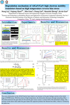
This paper presents degradation of AlGaN/GaN high electron mobility transistors with time in HTRB experiments at the same bias. The experimental results show that drain-to-source current of AlGaN/GaN HEMTs after HTRB stress was obviously lower than that of the fresh devices. The maximum change of drain-to source current was up to 188 mA. The threshold voltage drifted forward and gate-lag characteristic became worse for the AlGaN/GaN HEMTs after HTRB stress. The dependence of threshold voltage (Vth), capacitance-voltage (C-V), double pulse output curve and gate leakage current (Igd, Igs) on HTRB time was revealed at different time intervals. By analyzing the capacitance-voltage characteristic curves, the constant capacitance of forward bias is usually related to the SiNx capacitance, while the reverse bias depends on the total capacitance (Ctotal) of the SiNx layer and AlGaN [10], our experiments show that it is the SiNx layer that causes the change in capacitance.
The device under test (DUT) is AlGaN/GaN HEMT, as shown in Fig. 1. The Vds and Vgs bias waveform during the experiments are given in figure. 2. In the past, many experiments were conducted with the same interval time, but the degradation process of the device is often a non-linear process, and the step length setting is very important. Too long step length may miss the time point of device mutation, while too short step length makes the results are affected by the test conditions, making the results inaccurate. In this experiment, we roughly determined the mutation range of the device through preliminary exploration. As we can see, to get a better view of results, the experiment step time was set to 10h, 30h, 60h, 100h, 200h, bias stress test (Vgstress = −10 V, Vdstress = 60 V), the experiment temperature was set to 150 ℃, in order to determine the failure time of the device, we used a computer program to control the applied stress and monitor the real-time current.
All virgin and stressed devices have been extensively characterized. For the purpose of clarity, we compare the original device with the device after 100 h and 300 h stress in Fig. 3 to indicate the changes of output transfer and characteristics. It can be seen from the figure that the threshold voltage drifted forward before and after the stress, and the current collapsed worsen obviously, indicating that the device had a certain degree of degradation. However, the threshold voltage was almost unchanged from 100 h to 300 h, while the output current collapsed worsen. This phenomenon indicates that it is possible that AlGaN/GaN interface captures charge, leading to the reduction of channel carriers density, or it is possible that the increase of electron state density in SiNx/AlGaN or SiNx leads to the depletion of 2DEG to a certain extent and the decrease of output current. To shed a light on this, we did other tests.
Figure 4 shows the gate leakage current of the device at different stress stages. The gate source current decreases by 0.041 mA and the gate leakage current decreases by 0.0436 mA before and after the stress. Figure 5 is the gate delay curve before and after the stress. The device needs 30% more time to reach the maximum current. Figure 6 shows C-V characteristic curves after stress, we notice that the stretch-out effect of the curve decreases with time. The Fermi level (EF) is located far below the valence band maximum of AlGaN at the Al2O3/AlGaN interface, which makes electron occupation of interface states no longer a function of the gate bias, leading to absence of stretch-out behavior in the C-V curve [10].
Pulsed drain current versus drain voltage (ID- VD) measurements, carried out starting from several quiescent bias points in the off-state, may be used to quantitatively evaluate the current collapse, and to characterize a specific device technology in terms of sensitivity to trapping processes. The pulsed IV waveforms examined can provide the capability of isothermal (constant temperature ) and isodynamic (constant trap occupancy) transistor measurements for more accurate RF characterization.
The difference on pulsed output characteristics in Fig. 7 is revealed for various quiescent conditions of Vgs-q. Similar plots have largely been reported in the literature related to GaN HEMT structures, as in [6], where (co)doping of the buffer is investigated as the cause for such signature. The current under pulse measurement is lower than that under DC test, and the current collapse appears. The static operating point is (Vgs-q, Vds-q)=(-4V, 0V), and the device is in the cut-off state.The Schottky gate /AlGaN interface state and the ungate AlGaN surface state can capture electrons and cause the current collapse phenomenon
关键词
high temperature reverse bias stress,interface trap state,electron state density
报告人

Meng Lu
Xiangtan University稿件作者
全部评论
重要日期
-
会议日期
08月25日
2021
至08月27日
2021
-
04月21日 2021
摘要截稿日期
-
05月15日 2021
摘要录用通知日期
-
06月25日 2021
终稿截稿日期
-
08月24日 2021
报告提交截止日期
-
08月27日 2021
注册截止日期
主办单位
IEEE
IEEE ELECTRONIC DEVICE SOCIETY
IEEE ELECTRONIC DEVICE SOCIETY
承办单位
Huazhong University of Science and Technology
联系方式
- Dr. 刘老师
- li******@vip.163.com
历届会议
-
2025年08月15日 中国 Beijing
2025 IEEE Workshop on Wide Bandgap Power Devices and Applications in Asia -
2025年08月15日 中国 Beijing
The 2025 IEEE Workshop on Wide Bandgap Power Devices and Applications in Asia -
2023年08月27日 台湾-中国 Hsinchu
2023 IEEE Workshop on Wide Bandgap Power Devices and Applications in Asia -
2018年05月17日 中国 xian
IEEE Workshop on Wide Bandgap Power Devices and Applications in Asia


发表评论