报告详情
Design and Verification of Gate Driver for 6.5 kV SiC MOSFET Module
编号:30
访问权限:公开
更新:2021-07-21 20:02:09 浏览:1198次
张贴报告
摘要
Design and Verification of Gate Driver for 6.5 kV SiC MOSFET Module
Yijian Wang, Lin Liang, Hai Shang, Lubin Han
State Key Laboratory of Advanced Electromagnetic Engineering and Technology, School of Electrical and Electronic Engineering, Engineering Research Center of Power Safety and Efficiency, Ministry of Education, Huazhong University of Science and Technology, 430074 Wuhan, China
lianglin@hust.edu.cn
Purpose of work
In this paper, gate driver with low coupling capacitance for 6.5 kV/25A SiC MOSFET module is proposed. Compared with 6.5 kV Si IGBT module, 6.5 kV SiC MOSFET module can switch at a higher frequency, improving the power density greatly. However, the common mode current flowing through the coupling capacitance between primary and secondary sides of the isolation transformer produced by high dv/dt during fast switching may produce annoying EMI. So far, there is no commercial gate driver for 6.5 kV SiC MOSFET module. Low coupling capacitance and enough isolation are main challenges for gate driver for 6.5 kV SiC MOSFET module. Several design schemes of isolation transformer are proposed in [1] [2], such as square core transformer, ferrite toroidal core transformer, and transformer with PCB winding, et al. As for double galvanic isolation transformer developed in [1], it has lower coupling capacitance than single ring isolation transformer. However, its’ effectiveness is not verified by driving experiment. Therefore, the coupling capacitance comparison between these two schemes, attached with driving experiment verification, is implemented.
Approach
Fig. 1 shows the diagram of the gate driver for 6.5 kV SiC MOSFET module. Based on the isolation voltage, taking robust into consideration, the design of transformer is determined. To obtain low magnetizing current, the primary and secondary windings should have enough turns. Here, the turns of the primary winding are 4 and there are 16 and 12 turns on secondary windings, respectively. Ten layers of high voltage kapton tape are wrapped around the core to get good insulation between windings and the core. Ferrite toroidal core produced by TDK, HF60T62X13X39, is used to make isolation transformer of two schemes. Besides, SMA (Sub Miniature version A) connectors and RF coaxial line with very low lead inductance and resistance are used to decrease the signal distortion during the transfer path from date driver to the gate of the 6.5 kV SiC MOSFET module.
Results and Significance
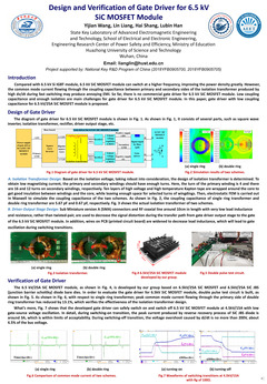
FEM (Electrostatic Finite Element) models are built to simulate the coupling capacitance of the two schemes. As shown in Fig. 2, the coupling capacitance of single ring transformer and double ring transformer are 5.67 pF and 0.67 pF, respectively. Fig. 3 shows the actual isolation transformer of two schemes. The 6.5 kV/25A SiC MOSFET module shown in Fig. 4 is developed by our group based on bare chip. In Fig. 5, double pulse test is used to evaluate the designed gate driver. As shown in Fig. 6, with respect to single ring transformer, peak common mode current flowing through the primary side of double ring transformer has reduced by 13.1%, which verifies the effectiveness of the design. Fig. 7 shows that the developed gate driver can switch off and switch on 6.5 kV SiC MOSFET module at 4.5kV/4A and 2kV/4A, respectively. During switching off, the voltage overshoot is less than 350V, about 7.8% of the bus voltage. It should be noted that the current oscillation during switching on is caused by 6.5kV/250A Si diode used in double test circuit, which limits the experiment at a higher voltage.
[1] K. Mainali, et al, "Design and evaluation of isolated gate driver power supply for medium voltage converter applications," in 2016 IEEE Applied Power Electronics Conference and Exposition (APEC), Long Beach, CA, USA, 2016, pp. 1632-1639.
[2] T. Batra, et al, "Isolation design considerations for power supply of medium voltage silicon carbide gate drivers," in 2017 IEEE Energy Conversion Congress and Exposition (ECCE), Cincinnati, OH, 2017, pp. 2552-2559.

Fig. 1 Diagram of gate driver for 6.5 kV SiC MOSFET module
Yijian Wang, Lin Liang, Hai Shang, Lubin Han
State Key Laboratory of Advanced Electromagnetic Engineering and Technology, School of Electrical and Electronic Engineering, Engineering Research Center of Power Safety and Efficiency, Ministry of Education, Huazhong University of Science and Technology, 430074 Wuhan, China
lianglin@hust.edu.cn
Purpose of work
In this paper, gate driver with low coupling capacitance for 6.5 kV/25A SiC MOSFET module is proposed. Compared with 6.5 kV Si IGBT module, 6.5 kV SiC MOSFET module can switch at a higher frequency, improving the power density greatly. However, the common mode current flowing through the coupling capacitance between primary and secondary sides of the isolation transformer produced by high dv/dt during fast switching may produce annoying EMI. So far, there is no commercial gate driver for 6.5 kV SiC MOSFET module. Low coupling capacitance and enough isolation are main challenges for gate driver for 6.5 kV SiC MOSFET module. Several design schemes of isolation transformer are proposed in [1] [2], such as square core transformer, ferrite toroidal core transformer, and transformer with PCB winding, et al. As for double galvanic isolation transformer developed in [1], it has lower coupling capacitance than single ring isolation transformer. However, its’ effectiveness is not verified by driving experiment. Therefore, the coupling capacitance comparison between these two schemes, attached with driving experiment verification, is implemented.
Approach
Fig. 1 shows the diagram of the gate driver for 6.5 kV SiC MOSFET module. Based on the isolation voltage, taking robust into consideration, the design of transformer is determined. To obtain low magnetizing current, the primary and secondary windings should have enough turns. Here, the turns of the primary winding are 4 and there are 16 and 12 turns on secondary windings, respectively. Ten layers of high voltage kapton tape are wrapped around the core to get good insulation between windings and the core. Ferrite toroidal core produced by TDK, HF60T62X13X39, is used to make isolation transformer of two schemes. Besides, SMA (Sub Miniature version A) connectors and RF coaxial line with very low lead inductance and resistance are used to decrease the signal distortion during the transfer path from date driver to the gate of the 6.5 kV SiC MOSFET module.
Results and Significance
FEM (Electrostatic Finite Element) models are built to simulate the coupling capacitance of the two schemes. As shown in Fig. 2, the coupling capacitance of single ring transformer and double ring transformer are 5.67 pF and 0.67 pF, respectively. Fig. 3 shows the actual isolation transformer of two schemes. The 6.5 kV/25A SiC MOSFET module shown in Fig. 4 is developed by our group based on bare chip. In Fig. 5, double pulse test is used to evaluate the designed gate driver. As shown in Fig. 6, with respect to single ring transformer, peak common mode current flowing through the primary side of double ring transformer has reduced by 13.1%, which verifies the effectiveness of the design. Fig. 7 shows that the developed gate driver can switch off and switch on 6.5 kV SiC MOSFET module at 4.5kV/4A and 2kV/4A, respectively. During switching off, the voltage overshoot is less than 350V, about 7.8% of the bus voltage. It should be noted that the current oscillation during switching on is caused by 6.5kV/250A Si diode used in double test circuit, which limits the experiment at a higher voltage.
[1] K. Mainali, et al, "Design and evaluation of isolated gate driver power supply for medium voltage converter applications," in 2016 IEEE Applied Power Electronics Conference and Exposition (APEC), Long Beach, CA, USA, 2016, pp. 1632-1639.
[2] T. Batra, et al, "Isolation design considerations for power supply of medium voltage silicon carbide gate drivers," in 2017 IEEE Energy Conversion Congress and Exposition (ECCE), Cincinnati, OH, 2017, pp. 2552-2559.
 (a) (b) Fig. 2 Simulation results of two schemes (a) single ring (b) double ring |
 (a)  (b) Fig. 7 Waveforms of (a) turn off @4.5kV/4A (b) turn on @ 2kV/4A with Rg of 39Ω |
 (a)  (b) Fig. 6 Comparison of common mode current of two schemes (a) single ring (b) double ring |
|
Fig.4 6.5 kV/25 A SiC MOSFET module |
 Fig.5 Double pulse test circuit |
  (a) (b) Fig. 3 Isolation transformer (a) single ring (b) double ring |
关键词
SiC MOSFET,Gate Driver,Coupling Capacitance,Common Mode Current,Isolation Transformer
报告人

Yijian Wang
Huazhong University of Science and Technology稿件作者
全部评论
重要日期
-
会议日期
08月25日
2021
至08月27日
2021
-
04月21日 2021
摘要截稿日期
-
05月15日 2021
摘要录用通知日期
-
06月25日 2021
终稿截稿日期
-
08月24日 2021
报告提交截止日期
-
08月27日 2021
注册截止日期
主办单位
IEEE
IEEE ELECTRONIC DEVICE SOCIETY
IEEE ELECTRONIC DEVICE SOCIETY
承办单位
Huazhong University of Science and Technology
联系方式
- Dr. 刘老师
- li******@vip.163.com
历届会议
-
2025年08月15日 中国 Beijing
The 2025 IEEE Workshop on Wide Bandgap Power Devices and Applications in Asia -
2025年08月15日 中国 Beijing
2025 IEEE Workshop on Wide Bandgap Power Devices and Applications in Asia -
2023年08月27日 台湾-中国 Hsinchu
2023 IEEE Workshop on Wide Bandgap Power Devices and Applications in Asia -
2018年05月17日 中国 xian
IEEE Workshop on Wide Bandgap Power Devices and Applications in Asia


发表评论